Electronics Design Automation - KiCad Schematic Capture
BME254L - Spring 2026
Electronics Design Automation: Schematic Capture
Schematic Capture
UI/UX
Creating a Schematic
KiCad Documentation: Schematic Editing Operations
- Create a
New Project, which creates a schematic file.
DO NOT CHANGE THE GRID SPACING!!
Setup
Page Settings..., using semantic versionin forRevision.Configure
Schematic Setup..., includingProject:Net Classes.Place component / part (
Place Symbol) using default library. If component doesn’t exist, then you either need to:Download the part from an online database (e.g., SnapEDA)
Create part using the
Library Editor.
- Annotate components (give each component a unique label).
This is now done automatically in KiCad 8.x, but you may want to manually override some of the annotation defaults.
Assign component values
Label nets with meaningful names
Nets are like nodes; common voltage connections.
Use net labels to avoid connection chaos.
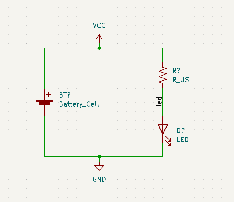
In-Class Exercise: Part I
Let’s create a simple voltage divider circuit…
Power Ports
Power ports, including ground references, are also global net labels.
Component pins can be explicitly designated power in/out (in contrast to signal).
Power, ideally, cascades top-to-bottom (
+\(\rightarrow\)GND[\(\rightarrow\)-]) on the schematic.
In-Class Exercise: Part II
Let’s add power ports…
Electrical Rules Check (ERC)
Check the validity of the schematic
Common error message:
“Input Power pin not driven by any Output Power pins”
KiCad checks to make sure that power can “drive” components that demand that input.
You can explicitly indicate this in the schematic using the
PWR_FLAGsymbol attached to the net in question.Might need to re-map pin types (
Properties:Edit Symbol:Pin Table).
Best Practices
Signal, ideally, flows left-to-right (input \(\rightarrow\) output).
Outline and label functional blocks. Use
Heirarchical Sheetsto organize more clearly-defined sub-circuits.Can include non-electrical items, like
Mounting Holes.Add Test Pins/Pads to nets you will want to verify during testing.
Power nets
Signal I/O
Use
No-Connectionflags for pins that are intentionally not connected to other components.
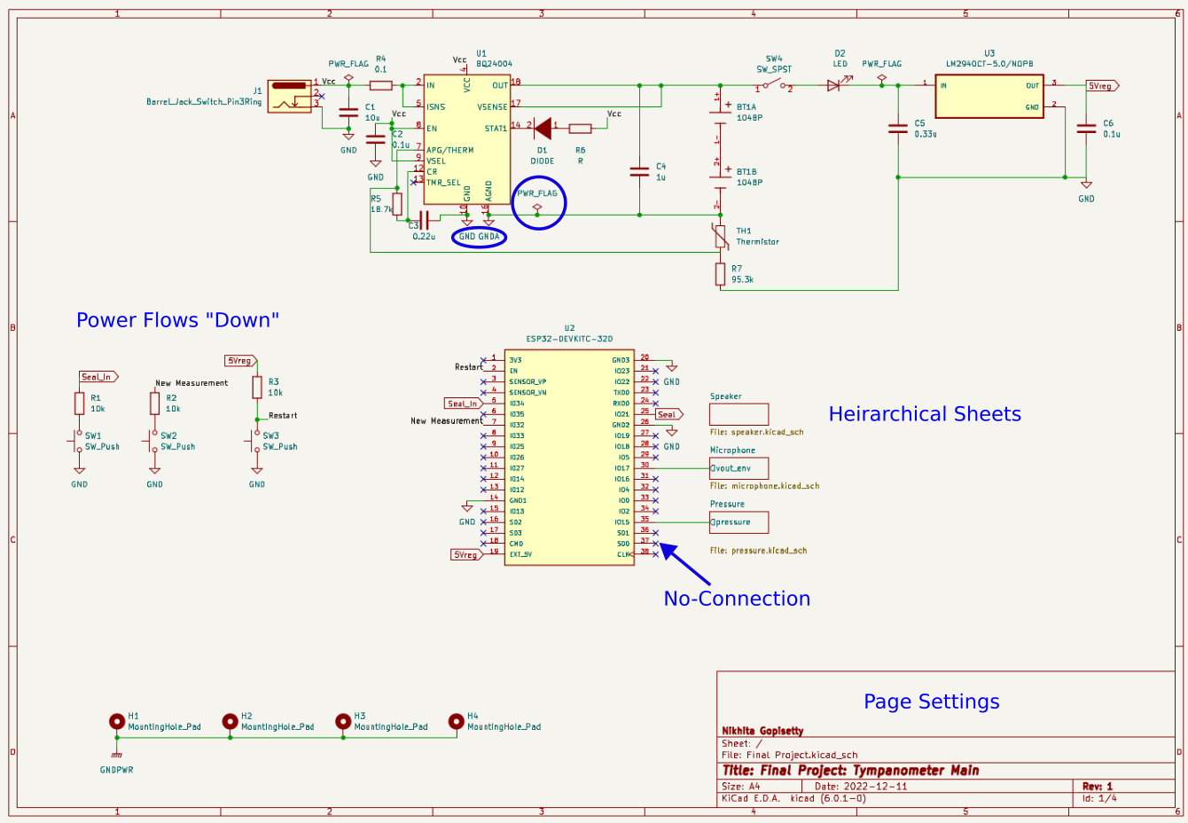
Schematic Components Not on the PCB
If a component will not exist on the PCB (e.g., a power switch, a control knob):
Be sure to exclude it from the board (
Properties\(\rightarrow\)General\(\rightarrow\) Exclude from Board).Represent the Connectors or Terminal Blocks on th schematic that will be used to connect the component to the PCB by wires.
In-Class Exercise: Part III
Modify your circuit to use a 9 V battert that will be connected to the PCB using a 2-pin connector.
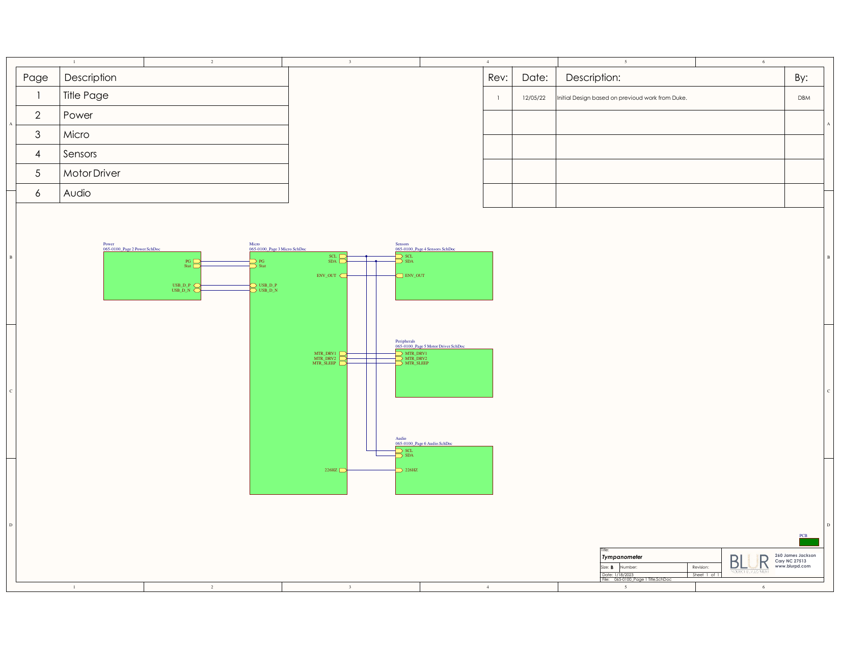
Heirarchecal Sheets
Circuits can get very complicated very quickly; quickly separated from functional signal flow.
Can organize functional sub-circuits into sheets (similar to writing functions in software development).
Sheets require explicit types of “pins” to allow signals to communicate between sheets.
Power ports are global and do not need to be explicitly connects.
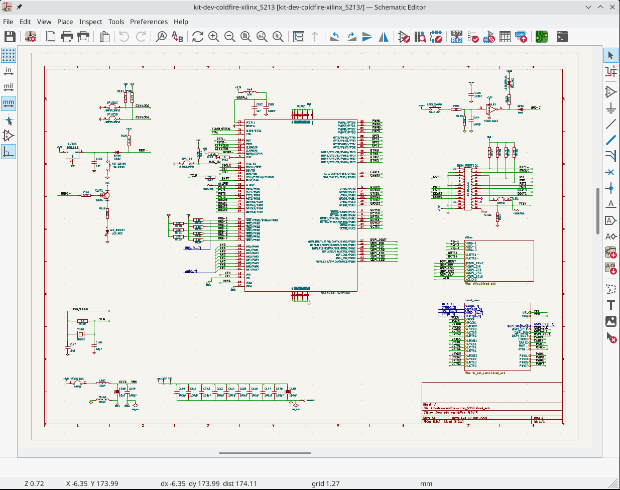
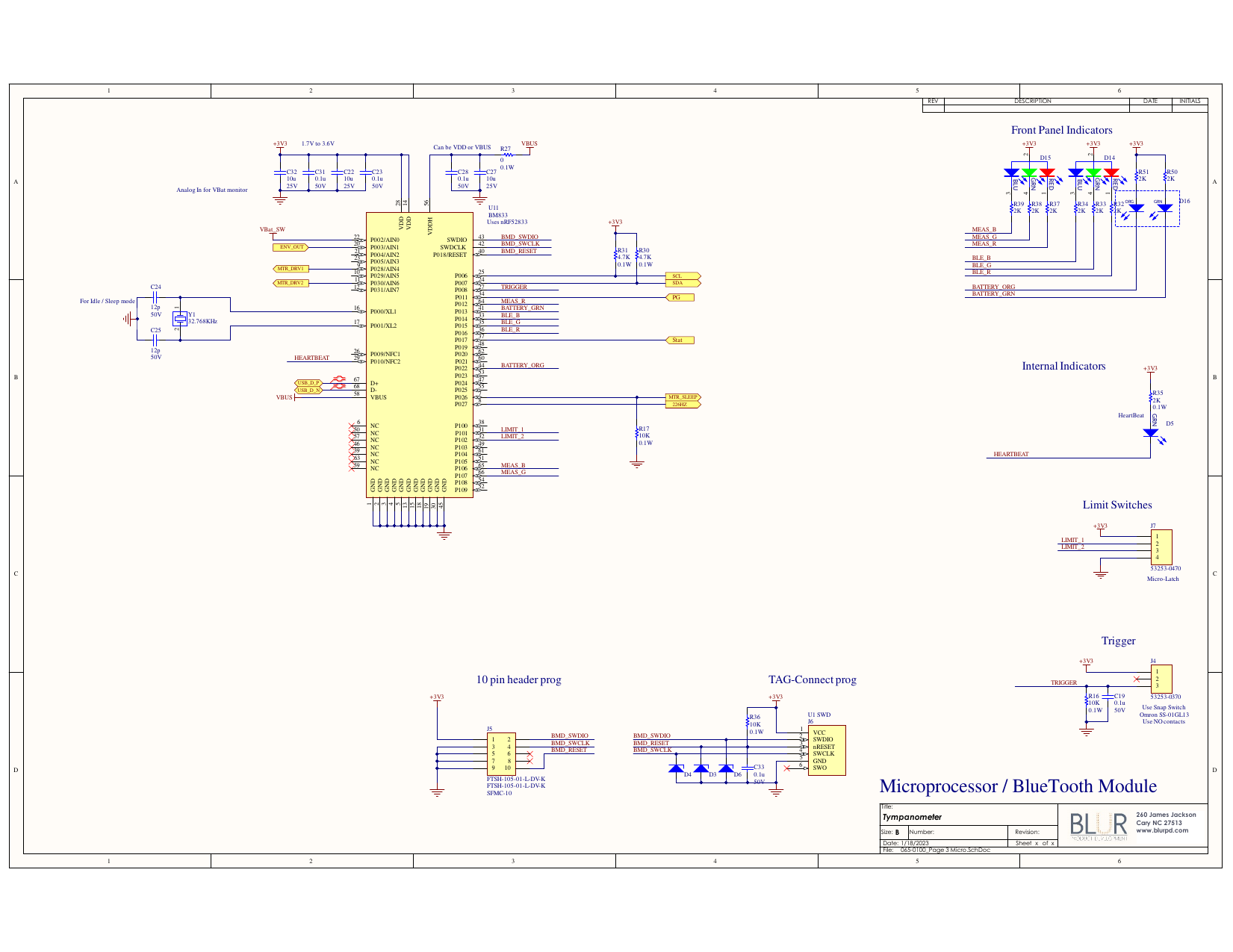
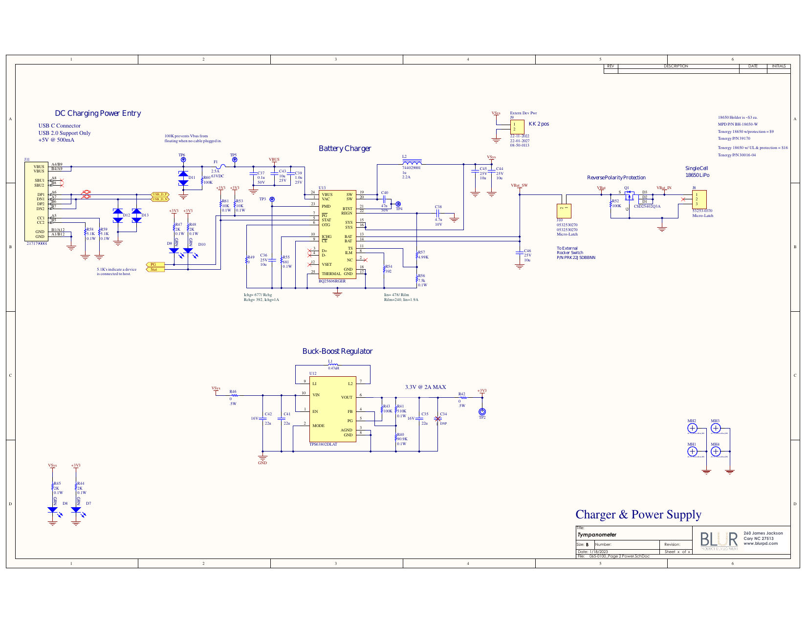
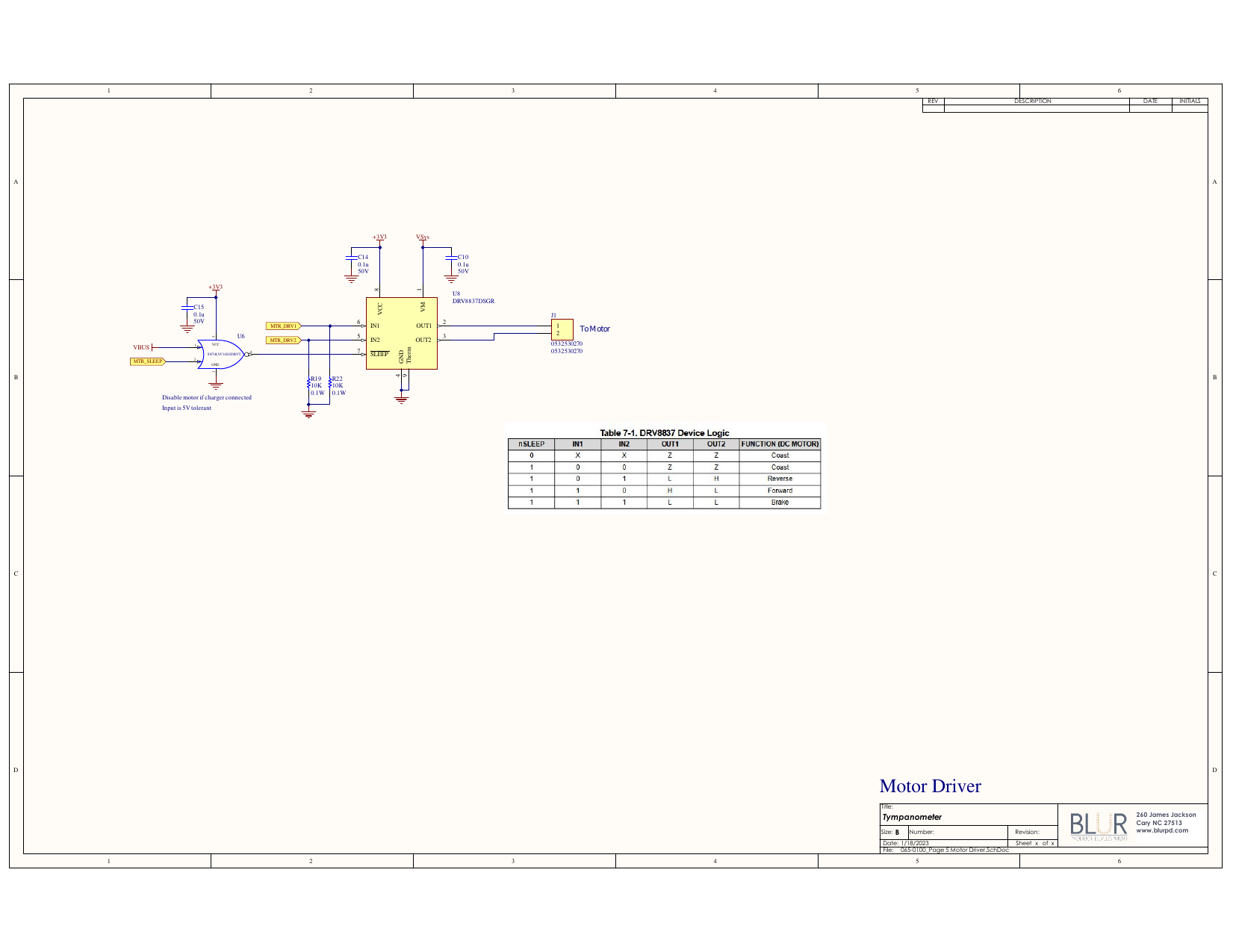
Example Project Schematic
Bill of Materials (BOM)
All of the components in the schematic can be populated into a Bill of Materials.
Industry-standard ECAD packages will be automatically linked to online part catalogs to order.
Components excluded from the board are still included in the BOM, unless explicitly excluded from the BOM (
Properties).
Troubleshooting
Certain video cards will not work well with the PCB tool. In that case, disable the
Acceleratedtoolset and choose theFallbackgraphics toolset.On Macs, your part / footprint / model libraries might not be detected automatically after installation. You might need to manually point Kicad at them in a path similar to:
Macintosh/Library/Application Support/kicad/templates/sym-lib-table/.