Electronics Design Automation - KiCad Schematic Capture
BME254L - Spring 2026
January 8, 2026
Schematic Capture
UI/UX
Creating a Schematic
KiCad Documentation: Schematic Editing Operations
- Create a
New Project, which creates a schematic file.
Warning
DO NOT CHANGE THE GRID SPACING!!
Setup
Page Settings..., using semantic versionin forRevision.Configure
Schematic Setup..., includingProject:Net Classes.Place component / part (
Place Symbol) using default library. If component doesn’t exist, then you either need to:Download the part from an online database (e.g., SnapEDA)
Create part using the
Library Editor.
Best Practices
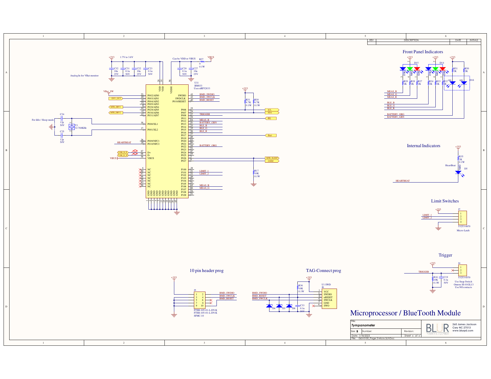
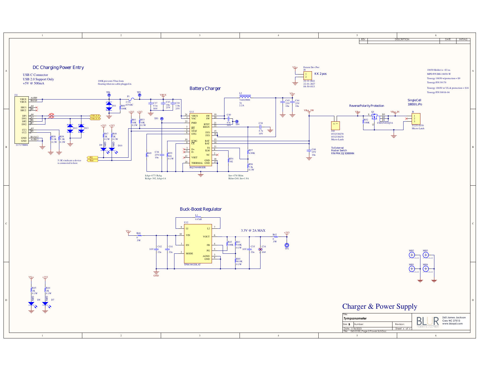
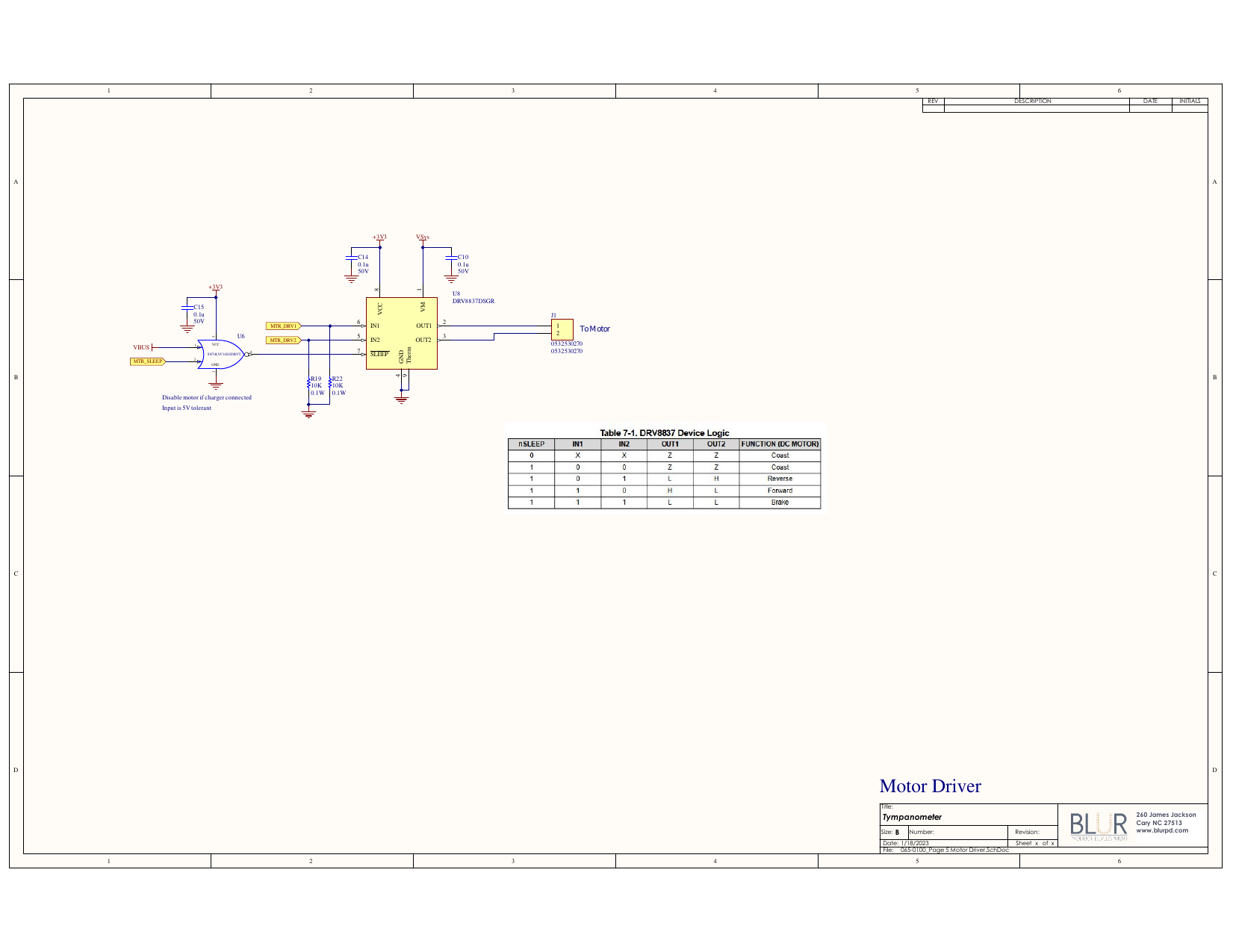
Signal, ideally, flows left-to-right (input \(\rightarrow\) output).
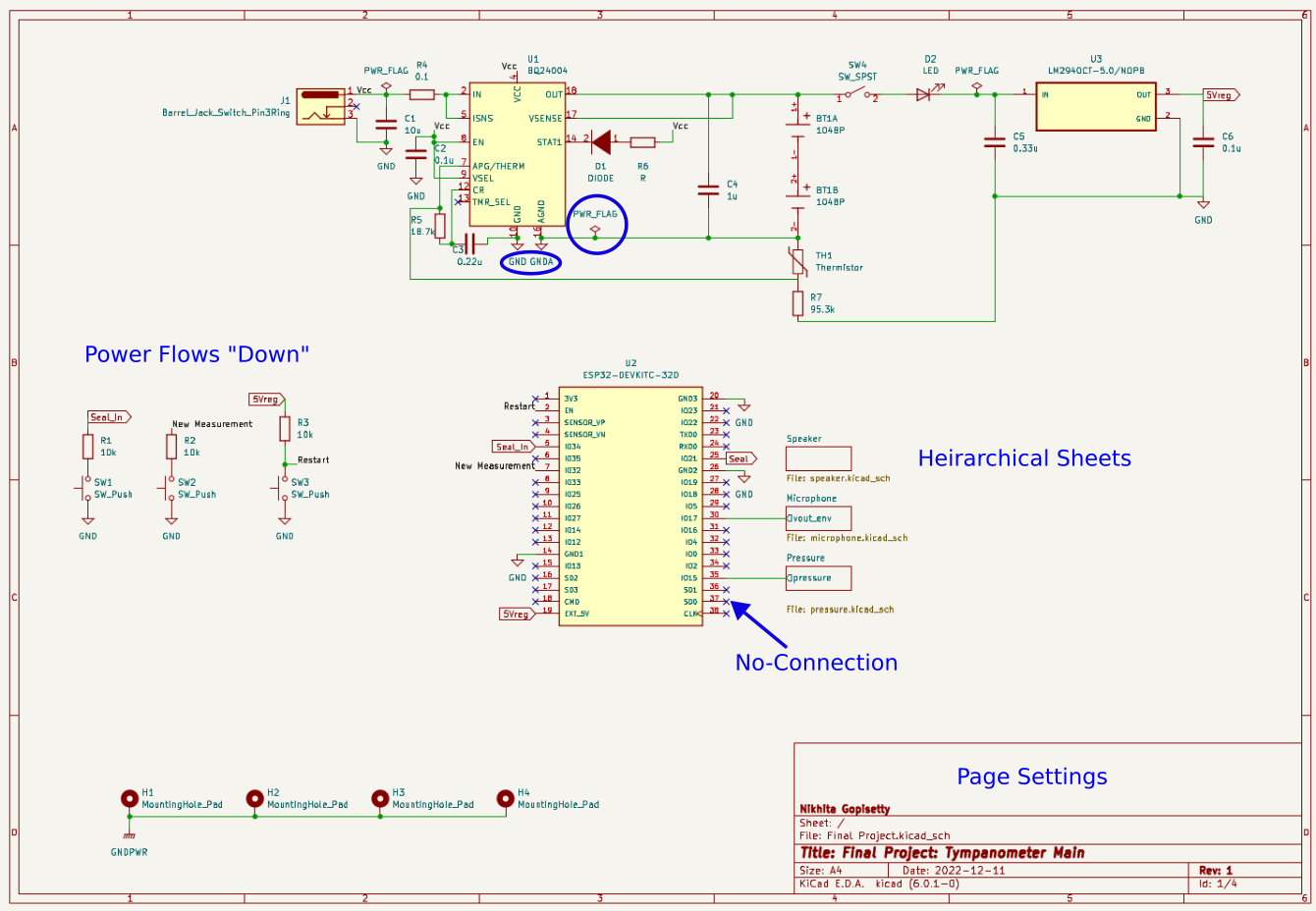
Outline and label functional blocks. Use
Heirarchical Sheetsto organize more clearly-defined sub-circuits.Can include non-electrical items, like
Mounting Holes.Add Test Pins/Pads to nets you will want to verify during testing.
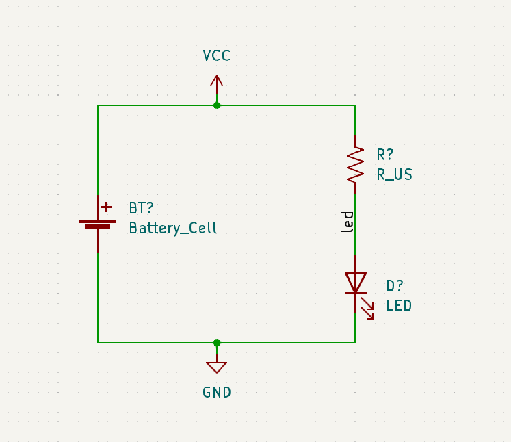
Power nets
Signal I/O
Use
No-Connectionflags for pins that are intentionally not connected to other components.
schematic_annotated
Schematic Components Not on the PCB
If a component will not exist on the PCB (e.g., a power switch, a control knob):
Be sure to exclude it from the board (
Properties\(\rightarrow\)General\(\rightarrow\) Exclude from Board).Represent the Connectors or Terminal Blocks on th schematic that will be used to connect the component to the PCB by wires.
In-Class Exercise: Part III
Modify your circuit to use a 9 V battert that will be connected to the PCB using a 2-pin connector.
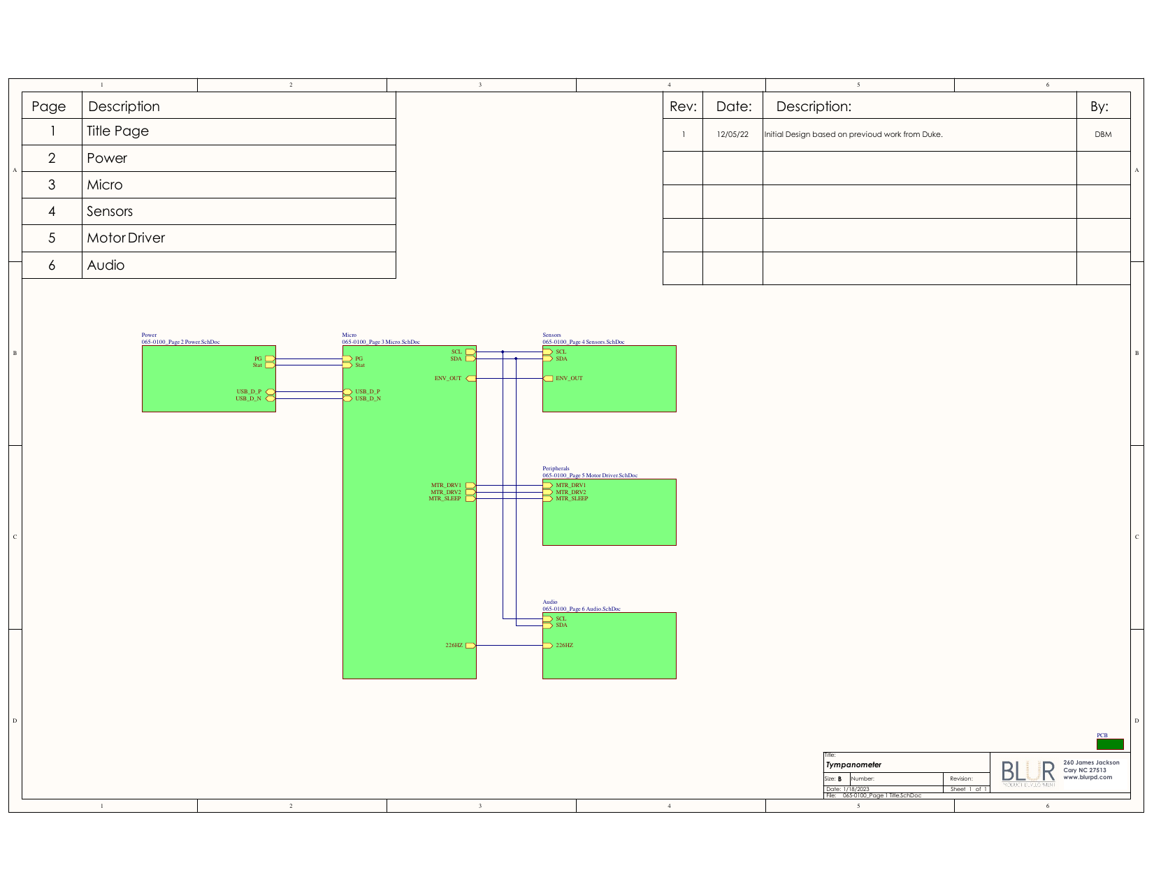
Heirarchecal Sheets
Circuits can get very complicated very quickly; quickly separated from functional signal flow.
Can organize functional sub-circuits into sheets (similar to writing functions in software development).
Sheets require explicit types of “pins” to allow signals to communicate between sheets.
Power ports are global and do not need to be explicitly connects.
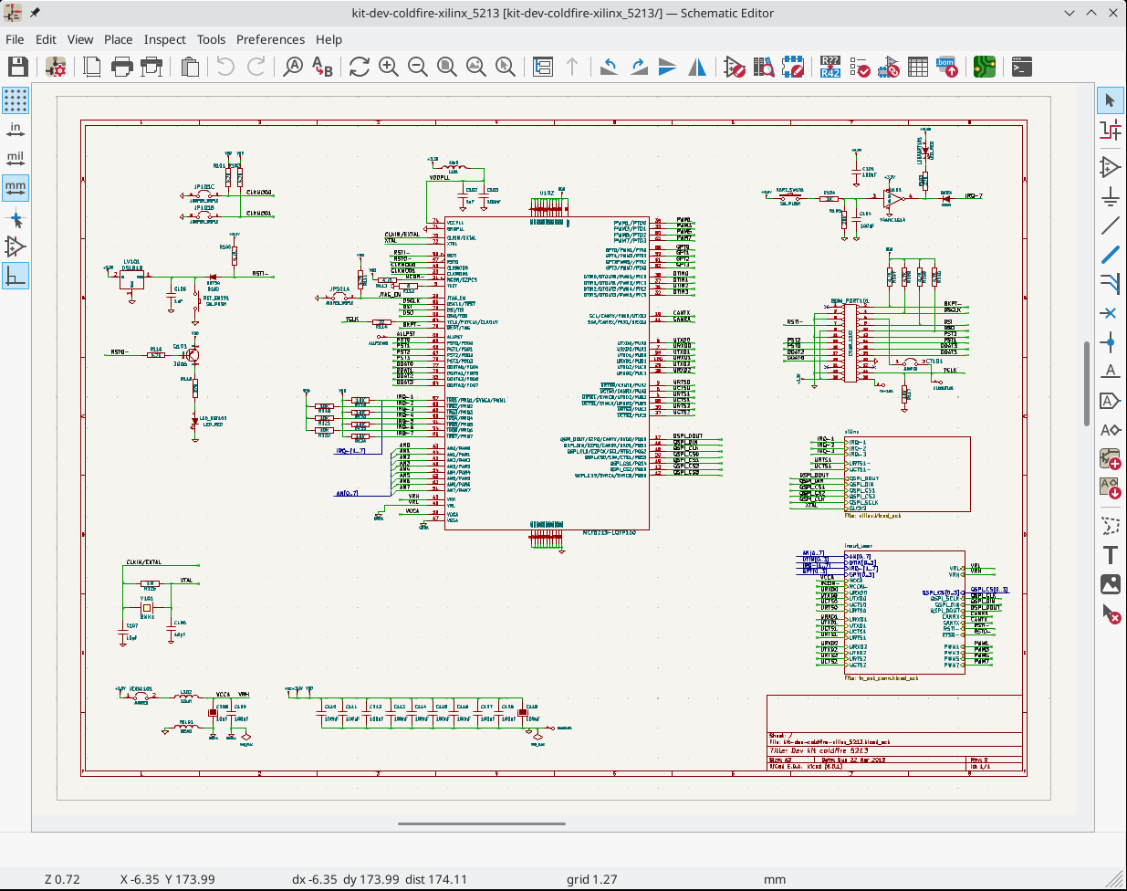
Example Project Schematic